


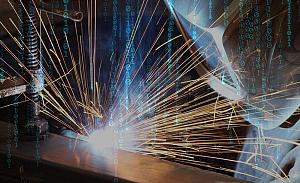
Additive manufacturing for electronics goes high end
The benefits of 3D-printing electronics are similar to those realized by printing other types of parts
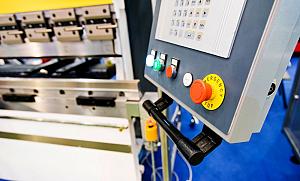
The ability to 3D-print conformal electronics could radically change the IC industry. nScrypt
I recently wrote in a blog posted to The Additive Report website that a sea change is underway in the printed circuit board (PCB) and integrated circuit (IC) industries, and that the future of electronics manufacturing is one in which companies will 3D-print “smart parts with embedded electronics.”
I also stated that we’re still in the pioneering stage of 3D-printed electronics, about where IC inventor Jack Kilby was a few years after applying for his patent on the Miniaturized Electronic Circuit in 1958.
It turns out I was wrong. The future described in the blog is already here, and it comes with a shiny new acronym: AME, short for additively manufactured electronics.
Electrifying Additive Manufacturing for Electronics
“AME allows a manufacturer to 3D-print complex circuitry such as that found in sensors and antennae in a single, seamless process,” said Valentin Storz, vice president of marketing and general manager of the Europe/Middle East/Africa region for Sunrise, Fla.-based Nano Dimension USA Inc.
The company’s DragonFly LDM (lights-out digital manufacturing) 3D printer jets conductive silver “nano ink” mixed with a polymer-based dielectric through dual printheads onto a nonconductive substrate. Storz said the ink, used to create electrical pathways, is deposited in layers 300 nm high and traces 110 microns wide, and the dielectric material is applied at a thickness of 2.5 microns or greater.
Up to 50 alternating layers can be printed on a single circuit, allowing for the construction of coils, capacitors, filters, and other embedded components that normally would be inserted using an automated pick-and-place machine. And, unlike traditional PCB manufacturing methods, 3D printing eliminates etching, electroplating, and drilling.
Vias (interlayer connections) and through-holes can be printed in whatever orientation is desired, and because the circuits can be stacked and interconnected atop one another, the component density is potentially much higher, as is the possibility of working on nonplanar surfaces.
Storz refers to these next-generation PCBs as high-performance electronic devices, or Hi-PEDs. “We call them that because this technology enables electronics manufacturers to do so much more than is possible with a conventional PCB,” he said. “Since you’re not bound to planar sheets, you can build and embed components such as capacitors, coils, and even MEMS devices. In traditional IC and PCB manufacturing, each additional layer adds complexity and cost, limiting how high you can go. For us, as with so many other additive processes, complexity is free.”
Dispensing With Convention
Kenneth Church agrees. The CEO of nScrypt Inc., Orlando, Fla., said additively manufactured electronics have been in the works for more than two decades.
In the late ’90s, his R&D firm Sciperio (the parent company of nScrypt) and other organizations participated in a DARPA-sponsored “coopetition” to fabricate mesoscale electronics, with the intent being to bridge the gap between macro- and micro-manufacturing processes. They called the program Mesoscopic Integrated Conformal Electronics (MICE).
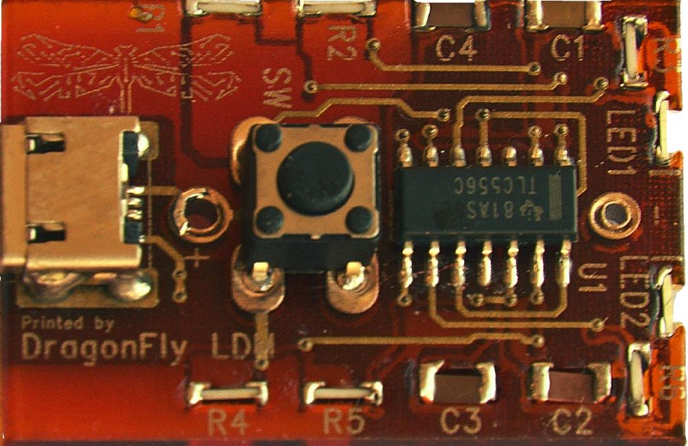
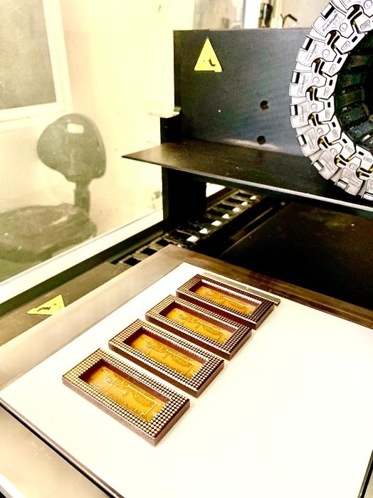
Nano Dimension’s DragonFly printer jets conductive silver “nano ink” mixed with a polymer-based dielectric through dual printheads onto a nonconductive substrate. Nano Dimension
The collaborative effort led to development of numerous direct-write 3D printing technologies that now go head to head in the industrial marketplace. nScrypt’s precision microdispensing and direct-digital manufacturing are an outgrowth of MICE.
Church described a significantly different manufacturing approach than that used by Nano Dimension. nScrypt’s Factory in a Tool (FiT) is an FDM-style printer boasting a “palette” of 10,000-plus materials. Unlike most 3D printers, however, this one is a hybrid. It comes with a high-speed machining spindle and automatic tool changer, and it can pick and place any electronic component that can’t be 3D-printed. With FiT, there’s also the option of in-process sintering, UV curing of polymers, machine vision, and laser integration.
Depending on the material, FiT can print conductive lines and dots as small as 20 microns and 50 microns, respectively, while also conforming to rough or curved surfaces.
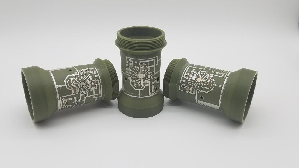
“In one recent example, we worked with the U.S. Air Force to construct 3D-printed phased-array antennas containing seven layers of RF circuitry, and then simply printed a quadcopter around them,” Church said. “We’ve also developed a range of 3D-printed ‘circuit cylinders’ with electronics embedded in the walls. These are very robust, can be tuned to specific applications, and completely eliminate the need for PCBs.”
Equipment specifics and manufacturing capabilities aside, Storz and Church concur that the market for AME is building rapidly. Church points to studies estimating it will grow to “somewhere north of $3 billion” over the next few years, and Nano Dimension’s Stolz estimated the growth rate for wearables and flexible electronics is roughly twice that of traditional PCB manufacturing.
Given its greater design freedom, accelerated time to market, and far lower tooling costs, 3D printing is the most effective way to meet the needs of high-end electronics manufacturers.
Tooling in Additive Manufacturing for Electronics
Despite 3D printing’s effectiveness, it’s clear that conventional PCBs and ICs aren’t going away anytime soon, and that means neither will the tooling needed to make them. Here again, though, 3D printing is playing an increasingly important role.
“In a typical PCB shop, a technician might spend hours sitting at a bench, manually applying tape to mask off certain areas of a board in preparation for conformal coating,” explained Garrett Harmon, applications engineering manager at Essentium Inc. “We can print custom, reusable masks from electronics-friendly materials like ESD [electrostatic discharge]-safe TPU in a fraction of the time and use them for longer than traditionally manufactured masks.”
The Austin, Texas, company’s line of High Speed Extrusion printers, though not specific to printing electronics, find broad use in the industry. Aside from the conformal coating masks mentioned, there are board-specific pallets and trays needed to transport PCBs through the manufacturing process, as well as a host of jigs, fixtures, racks, and guides.
“The funny thing about manufacturing, especially in the electronics industry, is that people are always looking for these huge, complex projects to justify investment in a 3D printer,” said Harmon. “But to me, it’s all these small, everyday components like masks and pallets and such that might otherwise add significant costs to the product and days or even weeks to the lead time. It’s here that AM often has the biggest impact.
“People don’t always see that right away, but once they have a 3D printer on their floor and have time to start playing around with it, they quickly wonder how they ever lived without one,” said Harmon.
About the Author

Kip Hanson
About the Publication
- Podcasting

In this episode of The Fabricator Podcast, Caleb Chamberlain, co-founder and CEO of OSH Cut, discusses his company’s...
- Trending Articles