


Ask the Stamping Expert: How do metal formers stamp the unstampable?
Getty Images
Q: We have received a quote request from one of our largest customers for a high-volume, thin-gauge stainless steel part, but the feature sizes are too small to stamp for our comfort level. We’re afraid of the fragile punches and tiny die cavities that will be required in our tools, and the breakage, costly maintenance, and excessive downtime that are sure to happen. Do you have any advice for us before we turn down this “impossible” opportunity?
A: When faced with what seems like a component design nightmare, you might consider photochemical etching, also known as photochemical machining. Panel photochemical etching is an inexpensive way to fabricate a medium quantity of parts for evaluation before building a production tool.
The beauty of this process is that fine features are very routine, and small or large complex parts can be fabricated easily. Tooling costs are a fraction of the cost of hard tools, and design changes can be made quickly. Since the tooling is optically based, part complexity doesn’t drive a higher tool cost as it does in conventional stamping.
In addition, the process is burr-free and stress-free, so no additional distortion is introduced. Multitudes of tiny holes and features can be created at once, not punched progressively a set at a time. Tempered material can be etched—a challenge for hard tooling.
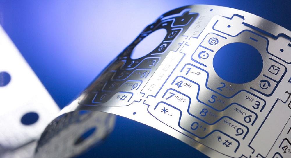
Potential feature sizes and tolerancing depend largely on raw material stock thickness. For convenience, ratios can be used for preliminary design. Hole diameters can be 1.2 times thickness or greater. Distance between features can be 1.0 times thickness or greater. The tolerance on some features can be as low as ± 5 µm, depending on feature size and material thickness. Etching a feature from one side only can produce a razor-sharp edge, flow channels, a half-etch connection for manual part removal, or text for permanent part identification.
Chemically etched metal is processed using techniques like those used in circuit board manufacturing. Both surfaces of the metal are coated with photoresist and placed between two pieces of patterned film or glass (depending on the accuracy required). The metal is exposed to UV light, and when the material is developed, unexposed resist is removed to create bare metal areas that etching removes. After etching, the remaining resist is removed, and the finished part is cleaned and dried.
This process really shines when continuous or reel-to-reel etching is employed. This method uses the same steps as in panel etching but can process continuous coils of stock, just like a progressive stamping die. Multiple strands can be produced at once and then wound onto reels. These reels can then be used for follow-on operations like plating, forming, molding, or welding. This is an economical method for high-volume production of complex metal parts and especially suited to trouble-free assembly of downstream processing and automation.
Photochemical etching can be used for common applications not readily possible with other fabrication methods:
- Filters and sieves with unusual shapes and extremely high open areas of precise, fine holes
- Flat springs from hard, thin material in complex shapes
- Laminated plates for spray nozzles, and heat exchangers or fuel cell plates using half-etched channels
This fabrication technology is not limited by application industry. Manufacturers in the automotive, medical, electronics, aerospace, and consumer devices industries often employ this technique to their advantage.
Many thanks to Domenic Federici, manager-business development with Interplex Etch Logic in Attleboro, Mass., for his assistance with this response.
About the Author

Thomas Vacca
Micro Co.
About the Publication
subscribe now
The Fabricator is North America's leading magazine for the metal forming and fabricating industry. The magazine delivers the news, technical articles, and case histories that enable fabricators to do their jobs more efficiently. The Fabricator has served the industry since 1970.
start your free subscription- Stay connected from anywhere
Easily access valuable industry resources now with full access to the digital edition of The Fabricator.

Easily access valuable industry resources now with full access to the digital edition of The Welder.
Easily access valuable industry resources now with full access to the digital edition of The Tube and Pipe Journal.
Easily access valuable industry resources now with full access to the digital edition of The Fabricator en Español.
- Podcasting

In this episode of The Fabricator Podcast, Caleb Chamberlain, co-founder and CEO of OSH Cut, discusses his company’s...
- Trending Articles
1
AI, machine learning, and the future of metal fabrication

2
Employee ownership: The best way to ensure engagement

3
Dynamic Metal blossoms with each passing year

4
Steel industry reacts to Nucor’s new weekly published HRC price
5
Metal fabrication management: A guide for new supervisors