


Manager, Advanced Technology
Connecting conductive parts to achieve electrical contact is one of the oldest, most ubiquitous joining applications. Required in almost every industry, the technologies used to make these connections are driven by cost, joint performance, and volume requirements.
As part miniaturization continues and connector sizes decrease to less than 0.004 in. thick for flat ribbons and wire diameters, traditional joining processes such as crimping, soldering, and brazing become less viable because of high joint resistance, questionable joint reliability, and unacceptable longevity. Welding, however, which provides excellent joint integrity, longevity, and conduction performance, is quickly becoming the required standard.
For joining two materials when at least one is less than 0.02 in. thick, the technology required is called microwelding. Copper is typically the material of choice for connecting conductive parts using microwelding because of its ability to conduct electrical energy and transmit signals. However, the very high thermal conductivity that makes copper such a good choice as a conductor rapidly pulls heat away from the weld joint, making it difficult to maintain heat balance and weld reliability. This difficulty is further exacerbated by trends toward increased production rates, reduced part size, and welding of dissimilar materials and dissimilar conductor cross sections.
The challenge of microwelding copper is controlling the heat balance in these small and highly conductive parts without over- or underheating. One way to overcome this significant challenge is to use a 532-nanometer (nm) wavelength. Because 532 nm lies within the visible light spectrum in the green wavelength band, it is also called “green.”
Microwelding copper conductive components can be done using ultrasonic bonding, resistance welding, and laser welding. Each has its advantages and disadvantages, and each meets microwelding requirements somewhat differently.
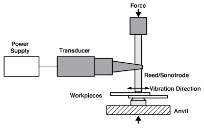
Ultrasonic Bonding. Well suited for sheet metal welding, particularly of conductive materials like copper and aluminum, ultrasonic bonding uses vibration energy at the joint interface to create the bond. The vibration energy is delivered to the interface by a sonotrode, or horn, that contacts the top workpiece (see Figure 1). The horn vibrates at frequencies of hundreds to thousands of times per second, with motion amplitude of 0.0005 to 0.004 in. The bottom workpiece is supported with an anvil, which can be either static or vibrating.
The vibratory action under applied force causes plastic deformation of surface disparities at the weld interface, leading to highly intimate contact and a diffusing of metallic atoms. The joint forms by diffusion, so there is no melting at the joint. Some deformation or thickness reduction occurs, but this can be controlled. The horn’s contact with the workpiece is maintained by the horn’s friction, enhanced by a knurling pattern on the horn along with a force applied on the workpieces.
The ultrasonic process has some drawbacks for microwelding. Since force is imparted onto the parts, mechanical contact is required on either side of the joint. Also, the horn is a consumable that requires inspection and replacement. Joint geometry is somewhat limited to lap welding only. Finally, the speed of the welding cycle that involves actuation of the horn can slow production rates.
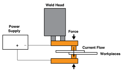
Resistance Welding. Resistance welding uses the weld interface’s high resistance to create heat as current is passed through the workpieces (see Figure 2). The circuit is created by electrodes that contact the workpiece either from the same side or opposite sides. Electrical contact is ensured by some force exerted on the parts.
During resistance welding on conductive parts, the electrodes are resistive and therefore perform two functions: They heat up and conduct heat to the workpieces, and they conduct sufficient current to enable some heating to occur at the joint interface.
Resistance welding works well for many joining applications and materials. However, because the process relies on mechanical contact and the need to create an electrical circuit between two electrodes, it may not work properly in all circumstances, especially if the workpieces are mechanically delicate. In addition, the minimum electrode diameter is about 0.04 in., which may limit joint accessibility.
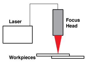
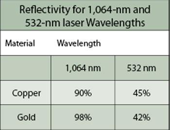
Laser Welding. Laser welding is a noncontact process requiring only single-sided access. The technology is useful for working in extremely small joint areas, and it can be used to weld different part shapes, different joint geometries, and dissimilar materials (see Figure 3). It uses no consumables that need to be maintained or replaced, and the weld cycle is milliseconds. On the face of it, laser welding appears to be an excellent solution for copper microwelding—but there is a problem. The pulsed Nd:YAG (neodymium-doped yttrium aluminum garnet) used for the majority of microwelding applications has a wavelength of 1,064 nm, which is more than 90 percent reflected by copper.
Extremely high power is required initially to overcome reflectivity and ensure that sufficient light energy is delivered to the copper. However, once some laser power is delivered to the copper and raises its temperature, the reflectivity decreases. As the absorption of laser power occurs in times scales of less than a billionth of a second, there is a rapid change in how much power is absorbed. The high power that was initially required now far exceeds what is needed to form the weld. As a result, the material overheats and vaporizes rapidly, leaving a large porosity or a hole.
A number of techniques have been used to overcome this reflectivity, including pulse shaping, oxygen assist, and using less reflective platings. Pulse shaping is not reliable because the reflectivity of copper and other conductive parts varies, and so the precise moment at which the laser power should be reduced also varies. Some attempts have been made to better anticipate this precise moment by implementing feedback techniques, but none have proven viable so far.
Oxygen has been shown to increase penetration in seam welding of copper by building an oxide layer on the part to be welded, but this has not been effective for spot welding applications because the positive effect of oxygen is seen only after several pulses in succession and so does not offer a reliable technique for single spot welding or short seams.
Using less reflective coatings such as nickel or tin does help to reduce initial reflection, but does not fully alleviate the problem as large energies are still required to continue the coupling into the copper. Thus, the process window for microwelding becomes very small.
As discussed, material reflectivity must be addressed to achieve a good, strong laser microweld on copper. By reducing the wavelength from 1,064 nm to 532 nm, the reflectivity of copper and other conductive materials decreases significantly (see Figure 4). The 532-nm green wavelength enables consistent coupling into the copper and stabilizes welding.
You can achieve this wavelength in two ways. First, use a Q-switched laser (which is most common); however, it does not have sufficient pulse energy to weld.
A more novel approach is to use a regular pulsed Nd:YAG laser, which offers 532-nm light at 1.5-kW peak power with up to a 5-millisecond pulse width. This provides enough weld energy to penetrate copper that is approximately 350 microns thick, which is sufficient for most microwelding applications.
Another benefit of using a pulsed Nd:YAG laser delivered through a fiber is that the beam has low brightness, which promotes even absorption across the focus spot, preventing hot spots at the center of the weld that may cause instability.
Electrical connections come in many different sizes, shapes, and materials and are found in many different industries. The welding of electrical contacts needs to be a seamless process that will allow the joint to perform as a single, solid, continuous component. For example, the automotive industry significantly increased its use of sensor technology to monitor car performance and functionality. Each sensor has many terminal connections that must survive for the lifetime of the car.
Connection requirements are also critical in the medical industry, for example, in implantable devices as well as sensing and monitoring instruments. Each connection is critical to maintaining part functionality and performance, and thus requires a highly stable joining technology. Similarly in the communications industry, signal strength and integrity are crucial to maximize part performance and ensure that the joint is not a limiting factor to the part’s design.
Microwelding conductive materials like copper is a difficult proposition, but laser welding offers a useful noncontact joining method, well geared for automation. In the past copper’s reflectivity at the 1,064-nm wavelength was always the barrier to implementing laser welding. A 532-nm green Nd:YAG laser welding system removes this barrier, thus offering a viable method for microwelding copper and other conductive materials in high volume.


The Welder, formerly known as Practical Welding Today, is a showcase of the real people who make the products we use and work with every day. This magazine has served the welding community in North America well for more than 20 years.
start your free subscription
Easily access valuable industry resources now with full access to the digital edition of The Fabricator.

Easily access valuable industry resources now with full access to the digital edition of The Welder.

Easily access valuable industry resources now with full access to the digital edition of The Tube and Pipe Journal.

Easily access valuable industry resources now with full access to the digital edition of The Fabricator en Español.
In this episode of The Fabricator Podcast, Caleb Chamberlain, co-founder and CEO of OSH Cut, discusses his company’s...


